Demands for energy conservation and the progress of information and communication systems are increasing. In response to these demands, we have developed a wide band gap semiconductor substrate with gallium nitride (GaN) as the next generation semiconductors.
GaN is widely used in blue light-emitting diodes due to its wide bandgap. Compared to conventional materials such as gallium arsenide (GaAs) or silicon (Si), GaN has a high electrical breakdown field, and a high electron mobility by stacking a heterojunction. GaN is hence greatly expected to be used as power transistors with high electron mobility.
These devices are now mostly manufactured by growing a single-crystal GaN film on different substrates, such as silicon carbide (SiC) and sapphire. However, due to the small area and high cost of SiC and sapphire, GaNs devices have been applied in limited markets only. CoorsTek therefore has developed a heteroepitaxial growth of a single-crystal GaN film on a large-area and inexpensive Si substrate.
| Concept: | By growing a single-crystal GaN film on a silicon substrate (Figure 1), we have been able to produce a semiconductor substrate which is large in area and inexpensive, for the next generation of devices. |
| Target: | For home appliances: Switching devices and invertors with hundreds of breakdown voltages. For mobile phone base stations: High power and high frequency transistors. |
| Advantages: | Our GaN on Si substrates are less costly than the other GaN on SiC or sapphire substrates, and it is possible to provide it in large diameters. Additionally, it is possible to use existing Si process lines. |
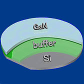
1. Image of GaN on Si substrates
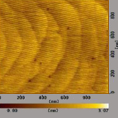
2. Surface morphology
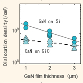
3. Density of defects
Komiyama, Jun, Yoshihisa Abe, Shunichi Suzuki, Toru Kita and Hideo Nakanishi. "Schottky diode characteristics of 3C-SiC grown on a Si substrate by vapor phase epitaxy." J. Crystal Growth, Vol. 275 (2005) e1001-e1006.
Abe, Yoshihisa, Jun Komiyama, Syunichi Suzuki and Hideo Nakanishi. "SiC epitaxial growth on Si(001) substrates using a BP buffer layer." J. Crystal Growth, Vol. 283 (2005) 41-47
Komiyama, Jun, Yoshihisa Abe, Shunichi Suzuki, Toru Kita and Hideo Nakanishi. "Suppression of crack generation in GaN epitaxy on Si using cubic SiC as intermediate layers." Applied Physics Letters, Vol. 88 (2006) 091901.
Komiyama, Jun, Yoshihisa Abe, Shunichi Suzuki and Hideo Nakanishi. "Stress reduction in epitaxial GaN films on Si using cubic SiC as intermediate layers." J. Applied Physics, Vol.100 (2006) 033519.
Komiyama, Jun, Yoshihisa Abe, Shunichi Suzuki, and Hideo Nakanishi. "Polarity of GaN films and 3C-SiC intermediate layers grown on Si substrates by MOVPE." J. Crystal Growth, Vol.298 (2007) 223-227.
Komiyama, J., K. Eriguchi, Y. Abe, S. Suzuki, H. Nakanishi, T. Yamane, H. Murakami, and A. Koukitu "Polarities of AlN films and underlying 3C-SiC intermediate layers grown on Si substrates." J. Crystal Growth, Vol. 310 (2008) 96-100.
Abe, Yoshihisa, Jun Komiyama, Syunichi Suzuki and Hideo Nakanishi. "Epitaxial growth 3C-SiC on Si(100) substrate using a BP buffer layer." The 20th General Conference of the Condensed Matter Division European Physical Society, Prague, Czech, Jul. (2004).
Komiyama, J., Y. Abe, S. Suzuki, T. Kita and H. Nakanishi. "Schottky diode characteristics of 3C-SiC grown on a Si substrate by vapor phase epitaxy." Fourteenth International Conference on Crystal Growth, ICCG14, Grenoble.
Komiyama, J., Y. Abe, S. Suzuki, and H. Nakanishi. "Preparation of cubic silicon carbide with smooth surface on carbonized porous silicon." Fall Meeting of The Electrochemical Society, USA (2004).
Komiyama, J., Y. Abe, S. Suzuki and H. Nakanishi. "Polarity of GaN films and 3C-SiC intermediate layers grown on Si substrates by MOVPE." 13th International Conference on Metal Organic Vapor Phase Epitaxy, ICMOVPE-XIII, Miyazaki.
Wide band gap:
Band gap refers to a field of energy formed through a band structure in crystals, and the field contains no electrons (semiconductor materials with a larger band gap than that of silicon are generally called wide band gap semiconductors). Materials which have a wide band gap possess good optical transparency, and they also have high electrical breakdown voltage.
Heterojunction:
The stack of different materials. Generally, in the field of semiconductors, relatively thin films of semiconductor materials that have different compositions are stacked. In the case of mixed crystals, heterojunctions with atomically flat interfaces and good interface characteristics is achieved. Owing to these interfaces, a layer of two-dimensional electron gas that has high electron mobility is generated.

