
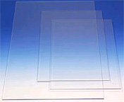

The T-4000 series of synthetic quartz glass boasts not only high purity, but also a great number of other highly desirable properties such as superior heat resistance, light transmittance, electrical insulation, and chemical stability. In addition, the properties of synthetic quartz glass and the advanced technology of polishing make photomask substrates suitable for exposure process of minute pattern in the manufacture of large liquid crystal displays (LCDs).

Large-scale photomask substrate
The synthetic quartz glass substrate with advanced polishing finish is shipped.
![]()
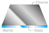
Blanks
Then, the chrome filme (shading film) is coated to make Blanks.
![]()
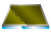
Resist Coating
Next, resist (exposure material) is applied onto the Blanks.
![]()
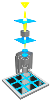
Drawing
The pattern is made with a drawing machine.
![]()

Developing
Then, the unnecessary resist is removed from the patterned mask.
![]()

Etching
Next, the unnecessary chrome is dissolved from the patterned mask.
![]()
Inspection/measuring
Finally, the patterned mask is inspected and measured.
![]()
Washing/shipping
After the mask passes inspection, it is washed with pure water and is shipped.